Sony releases new image CMOS sensor - IMX418
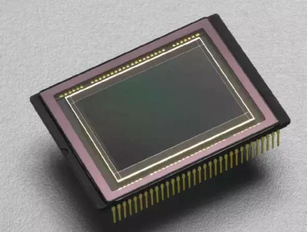
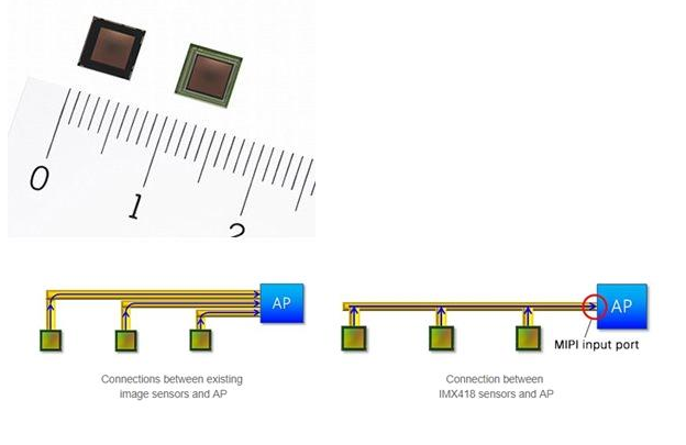
On October 22nd news, Sony today announced a new image CMOS sensor in Tokyo, IMX418. The IMX418 is the world's first image sensor that delivers signals from multiple sensors to the processor via the same MIPI interface in a "serial-like" manner. MIPI is the communication method between image sensor and AP/ISP. Usually, the former needs special cable and port to transmit information to the latter. If there are multiple sensors in the system, then route and open ports in sequence. On platforms where multiple IMX418 sensors are deployed, multiple signals can share a link and a port, passing the captured information in an orderly manner, which reduces the board area and allows plugging in the same size system in the past. Into more CMOS. The photosensitive element is the core of the camera and is also a key technology. At present, there are mainly two kinds of photosensitive elements: one is a CDD (Charge Coupled) element; the other is a CMOS (Complementary Metal Oxide Conductor) device. Although CCD imaging is more excellent, there are only a few manufacturers such as Sony. Panasonic and other masters of this technology, and its manufacturing process is complex, expensive, and CMOS manufacturing cost and power consumption is lower than CCD, so most of today's camera manufacturers use CMOS sensor, and it is Seen as the future imaging device, the sensors on the mobile phone are all CMOS sensors. In terms of specifications, the IMX418 is 1/3.6-inch in size and has 1 million effective pixels. It is equipped with a global shutter function without focal plane distortion. The price of a single chip is 1,500 yen, and the price of a package is 2,000 yen. It is reported that IMX418 will be mainly used in industrial markets, such as HMD head display equipment, automatic robots, etc. CMOS (Complementary Metal Oxide Semiconductor), a complementary metal oxide semiconductor, an amplifier component for voltage control, is the basic unit that constitutes a CMOS digital integrated circuit. The CMOS manufacturing process has also been applied to the production of photosensitive components for digital imaging equipment, especially for SLR digital cameras with large format specifications. The obtained image signal is converted into a digital signal output through an analog-to-digital converter (ADC) on the chip. The CMOS pixel size common to most mobile phones is now 1.12 microns, while the D800 pixel size as a single-lens reflex camera is 4.88 microns, and the photosensitive element is more than a multiple of the mobile phone. The size of the pixels is not fixed, and its order is not unique. For example, the general RGB sub-pixel arrangement, RGBW technology arrangement, Pentile arrangement, etc., this arrangement change can also improve the resolution and photographing experience of the picture, but more importantly, it depends on the size of the photosensitive element. Automatic Shape Moulding Machine With Vacuum Eps Shape Molding Machine,Insulated Eps Foam moulding machine,Automatic Eps Foam Machine,Fish Box Cooler Foam Machine Zhejiang Huasheng Machinery Equipment Co.,Ltd , https://www.hsfoammachine.com
