The level of nano-research in China has greatly increased into the international advanced ranks
On January 11, the Ministry of Science and Technology, the Chinese Academy of Sciences, and the Natural Science Foundation held a working meeting of the National Nanoscience and Technology Guidance Coordination Committee in Beijing. Wan Gang, the minister of science and technology, who is also the director of the committee, said at the meeting that the "Eleventh Five-Year Plan" for China's nanotechnology has achieved a leap-forward development, and the implementation of major research projects for nano-research has greatly enhanced the level of nano-research in China and entered the international advanced ranks. Has become a big nanotechnology country. Cao Jianlin, deputy director of the committee and deputy minister of science and technology, introduced that in recent years, China has implemented the "National Research Center for Nano Research" major national scientific research plan, the "863" plan, the National Natural Science Foundation of China, the special project of the State Key Laboratory, and the construction of a national science and technology infrastructure. Various talent special projects, etc. The total number of published nanotechnology papers exceeds that of the United States in the world, and the quality of the papers continues to increase. The papers have always been cited as the second highest frequency in the world; the number of patent applications for nanotechnology has ranked second in the world, and the standardization work for nanotechnology Synchronize with the international. Among them, many research results show broad prospects for promotion, laying the foundation for the industrialization and application of nanotechnology in China. Nanotechnology, information technology, and biotechnology together constitute the three pillars of today's world high-tech. It is understood that more than 50 countries and regions including the United States, Japan, the European Union and Russia all have their own development strategies for nanotechnology. The US National Nano Plan (NNI) 2011 budget of 1.8 billion U.S. dollars, annual investment in steady growth. Japan attaches particular importance to the application of nanotechnology in information, metals, environment, energy, life sciences, and basic technologies. In recent years, China has made breakthroughs in many aspects such as the development of nano-materials green printing plate making technology, bionics intelligent nano-interface materials, the preparation and performance of carbon nanotube macroscopic films and fiber structures, and nanostructured metal materials reaching high performance limits. According to the reporter’s understanding, the Ministry of Science and Technology is promoting the reform of scientific and technological plans and will use nanoscience and technology as a pilot. Under the framework of the Nanotechnology Guiding and Coordinating Committee, the coordination between departments and the Ministry of Science and Technology will be strengthened to promote the importance of nanotechnology research. The coordination and integration between the scientific research plan, the "863" plan, support plans, and other funding support channels will promote China's transformation from a large nanotechnology nation to a powerful nanotechnology nation.
The heavy-duty glass fibre reinforced plastic Durostone®and Glastic® offer extreme strength and excellent electrical, thermal and chemical properties. Durostone® pressed sheets meet the requirements of the EN 60893 standard. Durostone® and Glastic® are manufactured by using
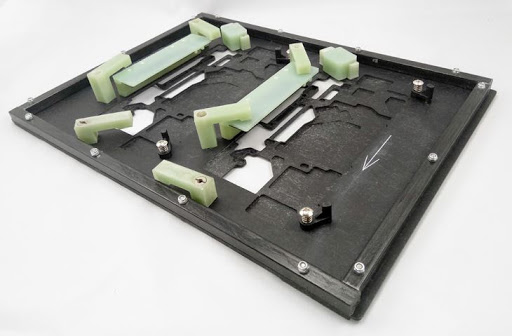
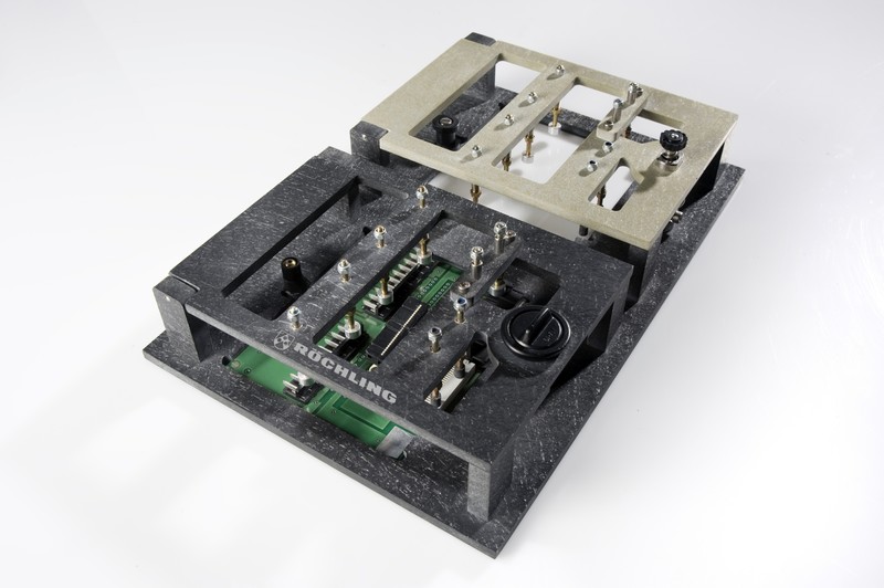
Wave Solder Pallet durostone range: The product range comprises sheets, composite profiles, wound components, compression molded parts and finished components of almost any type and size (up to 4 m [13.13 ft.] by 2.8 m [9.19 ft.]) for these applications.
Welding Pcb Reflow Solder Pallet Applications: Durostone® and Glastic® are especially well-suited for the use in generator construction, switchgear, chemicals processing equipment and transportation systems.
Durostone® materials have been developed for all procedures within the PCB assembly process. There are three main grades which are suitable for use in the SMT reflow and wave soldering processes
Durostone® is Produced in Three Standard Grades:
CHP 760 (Blue) (Standard)
CAS 761 (Black) (Anti-Static)
CAG 762 (Grey) (Anti-Static, Optical)
Antistatic durostone offer the following features:
Excellent mechanical properties at elevated temperatures including the lead-free process.Low thermal conductivity.Excellent machining properties enabling the manufacture of complex design solder pallets.Good resistance to chemicals used in modern fluxes.
FEATURES AND BENEFITS of Durostone® Wave Solder Pallet Material
All materials are dimensionally stable and retain their flatness through repeated cycling in the PCB assembly process.
The low thermal conductivity of Durostone® ensures optimal thermal distribution across the PCB.
The resin system used in Durostone provides resistance to the chemicals used in fluxes and also prevents solder pick-up.
Can be machined to tight tolerances.
For any inquiry , please contact sales@honyplastic.com or whatsapp +86 18680371609
Wave Solder Pallet durostone,Durostone®Glastic® Fibre reinforced materials,Welding Pcb Reflow Solder Pallet,Antistatic durostone,durostone Hony Engineering Plastics Co.,Ltd. , https://www.honyplastic.com

